CONDUCTIVE AFM PROBES
Though silicon is conducting in bulk due to the presence of the dopants, the surface of the probe is always coated by a thin (1 - 2 nm) native oxide film. That is why using the conductivity of Si probes for AFM measurements is only possible in UHV conditions after the film is removed.
For imaging of electric properties of materials in ambient conditions, probes with special conducting coatings are usually used.


DPE (LOW-NOISE)
PROBE
 DPE probe tip close-up
- 8 nm
- < 40 nm
- 40°
- 12 - 18 µm
- n-type silicon
- Platinum
- Platinum
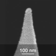
The DPE probe consists of a silicon tip and a special structure of conductive layers, which provides a more stable electrical signal and less noise. Because of the increase in tip radius, some reduction of resolution in the topography image is possible when using DPE probes in comparison with bare silicon probes due to the increased tip radius.
DPER (HIGH-RESOLUTION)
PROBE
 DPER probe tip close-up
- 8 nm
- < 20 nm
- 40°
- 12 - 18 µm
- n-type silicon
- Platinum
- Platinum
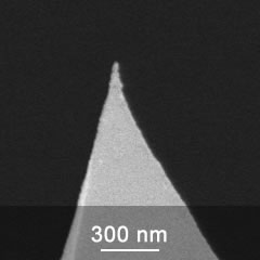
DPER probes are made by depositing a thin platinum coating on silicon tips. While the thickness of the coating on a flat cantilever surface is about 15 nm, there is only a 10 nm increase in the tip dimensions compared to bare silicon probes.
PT COATED
PROBE
 Pt coated probe tip close-up
- 8 nm
- < 30 nm
- 40°
- 12 - 18 µm
- n-type silicon
- Platinum
- Platinum
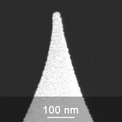
The pyramidal silicon etched probes with an overall conductive platinum coating are suitable for a wide range of electrical AFM applications. The platinum coating is a 30 nm thick film on both sides of the cantilever.
CR-AU COATED
PROBE
 Cr-Au coated probe tip close-up
- 8 nm
- < 35 nm
- 40
- 12 - 18 µm
- n-type silicon
- Gold
- Gold
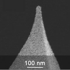
The Cr-Au coating is formed as a 30 nm Au film with a 20 nm Cr sublayer, which is deposited for better adhesion of Au. The coating is formed on both tipside and backside of the cantilever. The coating may cause cantilever bending within 3°.